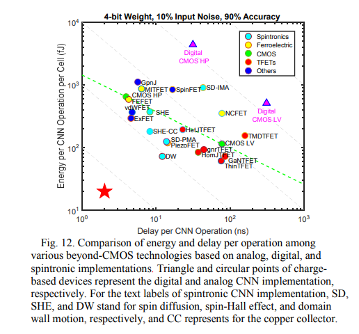
Energy - delay line for various junctions
practical devices need to be closer to the preferred corner - see the above picture (Fig. 12) from Wang-Kostner for the best processing performance on a single-cell level
- to measure in hbar? but still far too classical
2015 Benchmarking of Beyond-CMOS Exploratory Devices for Logic Integrated Circuits Dmitri E. Nikonov; Ian A. Young
see energy-delay line[1]
more references
Noel D’Souza 2018? Energy-efficient switching of nanomagnets for computing: Straintronics and other methodologies
Camsari 2016 Ultrafast Spin-Transfer-Torque Switching of Synthetic Ferrimagnets
Noel D'Souza 2014 Experimental Clocking of Nanomagnets with Strain for Ultra Low Power Boolean Logic
questions
- what is the basic physics expression for $ \lambda_{stt-mram} $? The parameter is not determined by the number of electrons in the nanomagnet cell, but rather being based on “collective physics” of (coupling to anisotropy, etc.), is it?
A: such an expression requires detailed equations
- how to square low-energy (small currents) spintronics (for instance, sensitivity of spin-diode) with the large dissipation of STT_MRAM relative to CMOS as expressed by $ \lambda_{STT-MRAM} $?
A: spin-diode does not have a tunneling barrier unlike stt-mram, so very different physics
- if $ \lambda_{STT-MRAM} $ remains large even as MtJ is shrinked in the "performance race", where does the energy will dissipate away from MtJ (otherwise overheating the junction)? In the case of CMOS, $ \lambda $ decreases as the cell size and number of electrons in the transistor decrease
A: ...
